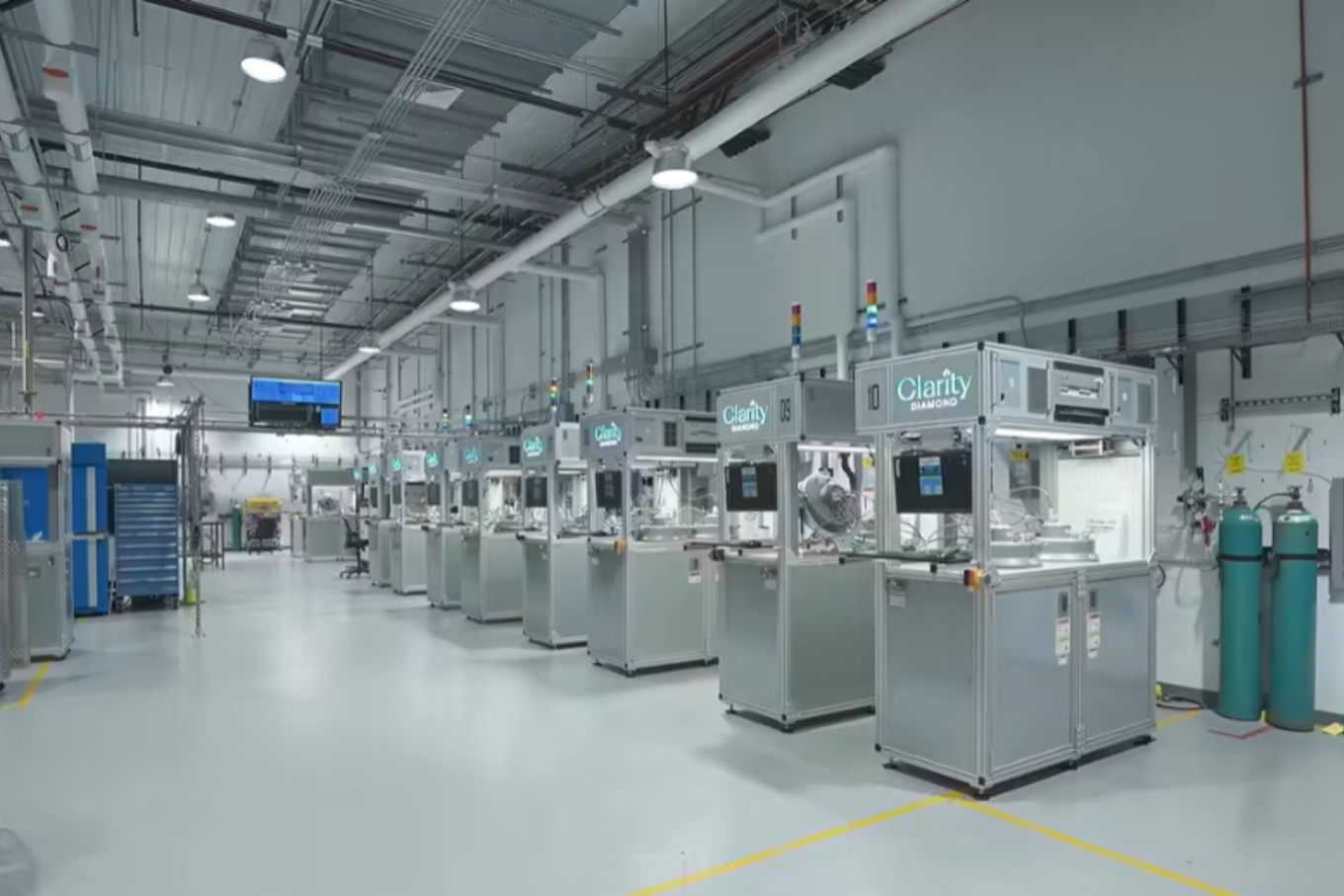
Most people, when they think of diamonds, picture jewellery or the hardened tips of industrial drill bits. Scientists and engineers have long known there is more to the story. Now, a convergence of advances in materials science, quantum physics, and semiconductor manufacturing is turning synthetic diamond into one of the most sought-after substances in high technology.
The diamonds in question are not mined. They are grown in laboratories, primarily through a process called chemical vapour deposition, or CVD. In CVD, carbon-rich gases such as methane are broken down under controlled conditions, and diamond crystals form layer by layer on a substrate. The result is a material with the same atomic structure as a natural diamond but produced with a precision that nature cannot match.
Why diamond beats silicon — and everything else
Silicon has underpinned the electronics industry for decades, but it has physical limits. As devices shrink and power densities rise, chips overheat, and silicon carbide and gallium nitride, two widely used alternatives, are reaching their own ceilings. Synthetic diamond offers properties that no other material can match at once: thermal conductivity more than five times higher than copper, an extremely wide electronic bandgap allowing it to withstand high voltages, and resistance to radiation, chemical attack, and extreme temperatures.
In power electronics, managing heat is the central challenge. Synthetic diamonds address this directly. Companies are now using synthetic diamonds as heat sinks in high-performance electronics including laser diodes, microprocessors, and high-power amplifiers. Data centres, which consume vast and growing quantities of energy partly because silicon-based chips require extensive cooling infrastructure, stand to benefit significantly from diamond-based thermal management.
‘Diamond wafers can now be employed using two of its extreme properties: extreme thermal performance plus extreme electrical insulation.’ — Diamond Foundry
In February 2025, Diamond Quanta published peer-reviewed results demonstrating exceptionally high electron mobility in polycrystalline diamond using a proprietary co-doping and defect engineering process, establishing for the first time an electronics-grade polycrystalline diamond platform with performance previously thought exclusive to single-crystal materials. Polycrystalline means the diamond is made up of many small crystals rather than one large one, which is far easier and cheaper to produce at scale.
The quantum dimension: sensing the invisible
Beyond power electronics lies a more exotic application. When a nitrogen atom replaces a carbon atom next to a vacant site in a diamond’s crystal lattice, it creates what physicists call a nitrogen-vacancy (NV) centre. This atomic-scale defect behaves as an isolated quantum system, and crucially, it can be read and manipulated at room temperature. Most other quantum computing approaches require cooling to near absolute zero, roughly minus 273 degrees Celsius, making them expensive and fragile. Diamond’s NV centres sidestep that requirement entirely.
NV centres make exceptional sensors. They can detect magnetic fields, electric fields, temperature, and pressure at the nanoscale with extraordinary precision. Researchers at the Hebrew University of Jerusalem, in collaboration with colleagues at Humboldt University in Berlin, have demonstrated near-optimal collection of single photons emitted by NV centres in a chip-based design, a result published in APL Quantum that supports future quantum computers, sensors, and communication networks. Solid-state quantum spins in diamond have demonstrated significant potential in quantum sensing, with applications ranging from fundamental science to medical diagnostics and navigation.
‘Diamond continues to shine — both literally and as a beacon for scientific and technological innovation.’ — Giuseppe Strangi, Case Western Reserve University
From laboratory to fabrication line
The central challenge has always been manufacturing. Growing diamond that is pure enough, large enough, and defect-free enough for semiconductor use is slow and expensive. Researchers at Princeton Plasma Physics Laboratory are working to grow diamond at lower temperatures than those currently used, a key step toward integrating it with existing silicon chip fabrication without damaging the silicon. In 2025, IonQ announced a breakthrough in synthetic diamond thin films that are quantum-grade and compatible with standard semiconductor fabrication techniques, allowing diamond to be integrated into photonic interconnects and devices in quantum systems.
A 2025 Quantum Diamond Workshop report identified a ‘diamond foundry platform’ and ‘quantum memories’ as critical technology gaps that, once closed, would unlock scalable fabrication. Despite impressive demonstrations that have reached advanced stages of technology readiness, the report noted that diamond technologies typically do not serve as straightforward replacements for existing materials but instead open entirely new applications.
A market taking shape
The broader synthetic diamond market was valued at roughly $27 billion in 2025 and is projected to reach $47 billion by 2036, growing at around five percent annually. Within that market, the CVD diamond segment focused specifically on electronics and thermal management is expanding far faster: the thermal management CVD diamond market alone was valued at $374 million in 2025 and is projected to reach nearly $1.8 billion by 2032, a compound annual growth rate of 25 percent. Electronics and semiconductor applications are creating new demand for CVD diamond substrates and heat dissipation components in high-power and quantum computing applications.
China leads in overall synthetic diamond manufacturing volume, while North American growth is increasingly supported by defence procurement and energy-efficient semiconductor initiatives. In Europe, Diamond Foundry has established a major wafer hub in Spain, and Germany’s machine-tool export sector has moved to standardise diamond tooling for electric-motor housings. The geopolitical dimension of advanced materials is never far from the surface: control of synthetic diamond manufacturing capacity is becoming a quiet but significant element of broader technology competition between major powers.
‘Electronics and semiconductor applications are creating new demand for CVD diamond substrates and heat dissipation components in high-power and quantum computing applications.’
The obstacles are real. Production costs remain high, achieving the defect densities required for semiconductor-grade material at commercial scale is technically demanding, and the industry lacks the decades of accumulated process knowledge that silicon benefits from. Yet the direction of travel is clear. Diamonds grown in a laboratory, atom by atom from carbon gas, are on course to become as important to the next generation of computing as silicon was to the last.
This article is free to read. It always will be — no paywall, no account, no tracking.